- 您现在的位置:买卖IC网 > Sheet目录490 > NTLJS1102PTBG (ON Semiconductor)MOSFET P-CH 8V 3.7A 6-WDFN
�� �
�
�NTLJS1102P�
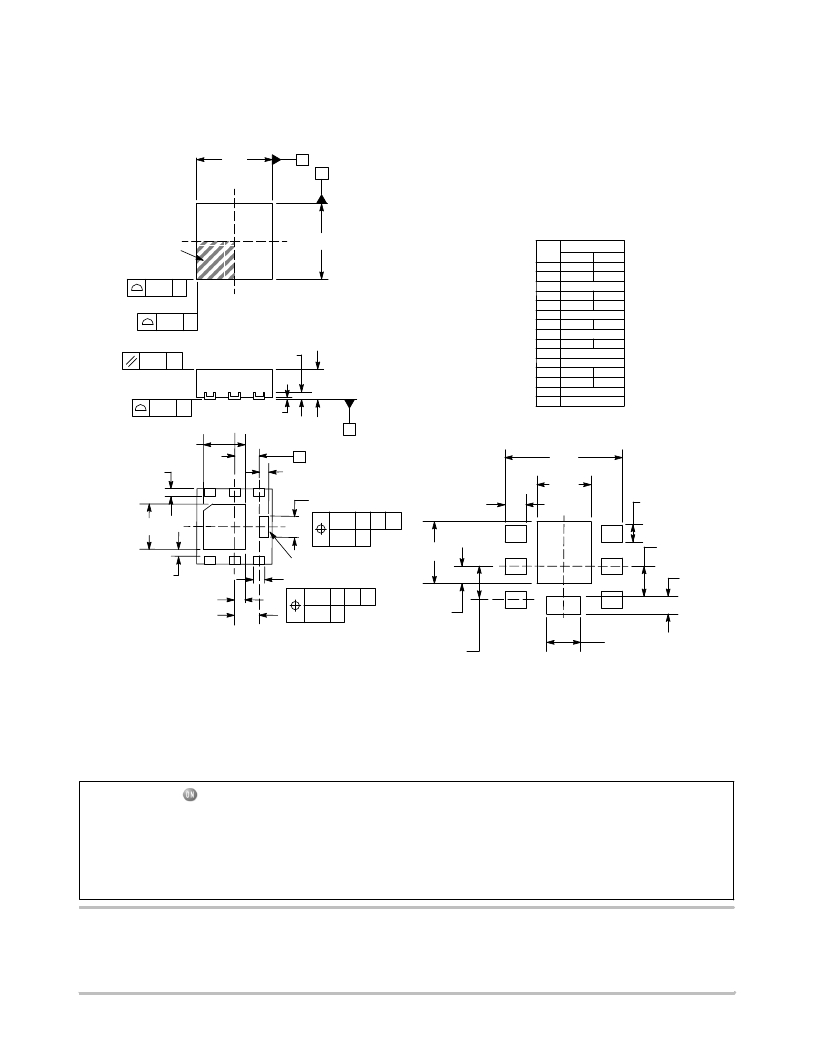
�PACKAGE� DIMENSIONS�
�WDFN6� 2x2�
�CASE� 506AP� ?� 01�
�ISSUE� B�
�NOTES:�
�1.� DIMENSIONING� AND� TOLERANCING� PER� ASME�
�D�
�A�
�B�
�Y14.5M,� 1994.�
�2.� CONTROLLING� DIMENSION:� MILLIMETERS.�
�3.� DIMENSION� b� APPLIES� TO� PLATED� TERMINAL� AND�
�IS� MEASURED� BETWEEN� 0.15� AND� 0.20mm� FROM�
�TERMINAL.�
�4.� COPLANARITY� APPLIES� TO� THE� EXPOSED� PAD� AS�
�WELL� AS� THE� TERMINALS.�
�5.� CENTER� TERMINAL� LEAD� IS� OPTIONAL.� TERMINAL�
�LEAD� IS� CONNECTED� TO� TERMINAL� LEAD� #� 4.�
�PIN� ONE�
�REFERENCE�
�E�
�6.� PINS� 1,� 2,� 5� AND� 6� ARE� TIED� TO� THE� FLAG.�
�MILLIMETERS�
�DIM� MIN� MAX�
�A�
�0.70� 0.80�
�A1�
�0.00� 0.05�
�2X�
�2X�
�0.10� C�
�0.10� C�
�A3�
�b�
�b1�
�D�
�D2�
�E�
�0.20� REF�
�0.25� 0.35�
�0.51� 0.61�
�2.00� BSC�
�1.00� 1.20�
�2.00� BSC�
�0.10� C�
�A3�
�A�
�E2�
�e�
�K�
�L�
�L2�
�J�
�1.10� 1.30�
�0.65� BSC�
�0.15� REF�
�0.20� 0.30�
�0.20� 0.30�
�0.27� REF�
�7X�
�0.08� C�
�A1�
�C�
�SEATING�
�PLANE�
�J1� 0.65� REF�
�SOLDERING� FOOTPRINT*�
�D2�
�4X�
�e�
�2.30�
�6X�
�L�
�1�
�3�
�L2�
�b1�
�6X�
�6X�
�0.43�
�1.10�
�6X�
�0.35�
�E2�
�K�
�6�
�4�
�b�
�NOTE� 5�
�6X�
�0.10� C� A�
�0.05� C�
�B�
�1.25�
�1�
�0.60�
�0.35�
�J�
�0.10� C� A�
�B�
�J1�
�BOTTOM� VIEW�
�0.05� C�
�NOTE� 3�
�0.34�
�0.65�
�PITCH�
�0.66�
�DIMENSIONS:� MILLIMETERS�
�*For� additional� information� on� our� Pb� ?� Free� strategy� and� soldering�
�details,� please� download� the� ON� Semiconductor� Soldering� and�
�Mounting� Techniques� Reference� Manual,� SOLDERRM/D.�
�m� Cool� is� a� trademark� of� Semiconductor� Components� Industries,� LLC� (SCILLC).�
�ON� Semiconductor� and� are� registered� trademarks� of� Semiconductor� Components� Industries,� LLC� (SCILLC).� SCILLC� reserves� the� right� to� make� changes� without� further� notice�
�to� any� products� herein.� SCILLC� makes� no� warranty,� representation� or� guarantee� regarding� the� suitability� of� its� products� for� any� particular� purpose,� nor� does� SCILLC� assume� any� liability�
�arising� out� of� the� application� or� use� of� any� product� or� circuit,� and� specifically� disclaims� any� and� all� liability,� including� without� limitation� special,� consequential� or� incidental� damages.�
�“Typical”� parameters� which� may� be� provided� in� SCILLC� data� sheets� and/or� specifications� can� and� do� vary� in� different� applications� and� actual� performance� may� vary� over� time.� All�
�operating� parameters,� including� “Typicals”� must� be� validated� for� each� customer� application� by� customer’s� technical� experts.� SCILLC� does� not� convey� any� license� under� its� patent� rights�
�nor� the� rights� of� others.� SCILLC� products� are� not� designed,� intended,� or� authorized� for� use� as� components� in� systems� intended� for� surgical� implant� into� the� body,� or� other� applications�
�intended� to� support� or� sustain� life,� or� for� any� other� application� in� which� the� failure� of� the� SCILLC� product� could� create� a� situation� where� personal� injury� or� death� may� occur.� Should�
�Buyer� purchase� or� use� SCILLC� products� for� any� such� unintended� or� unauthorized� application,� Buyer� shall� indemnify� and� hold� SCILLC� and� its� officers,� employees,� subsidiaries,� affiliates,�
�and� distributors� harmless� against� all� claims,� costs,� damages,� and� expenses,� and� reasonable� attorney� fees� arising� out� of,� directly� or� indirectly,� any� claim� of� personal� injury� or� death�
�associated� with� such� unintended� or� unauthorized� use,� even� if� such� claim� alleges� that� SCILLC� was� negligent� regarding� the� design� or� manufacture� of� the� part.� SCILLC� is� an� Equal�
�Opportunity/Affirmative� Action� Employer.� This� literature� is� subject� to� all� applicable� copyright� laws� and� is� not� for� resale� in� any� manner.�
�PUBLICATION� ORDERING� INFORMATION�
�LITERATURE� FULFILLMENT� :�
�Literature� Distribution� Center� for� ON� Semiconductor�
�P.O.� Box� 5163,� Denver,� Colorado� 80217� USA�
�Phone� :� 303� ?� 675� ?� 2175� or� 800� ?� 344� ?� 3860� Toll� Free� USA/Canada�
�Fax� :� 303� ?� 675� ?� 2176� or� 800� ?� 344� ?� 3867� Toll� Free� USA/Canada�
�Email� :� orderlit@onsemi.com�
�N.� American� Technical� Support� :� 800� ?� 282� ?� 9855� Toll� Free�
�USA/Canada�
�Europe,� Middle� East� and� Africa� Technical� Support:�
�Phone:� 421� 33� 790� 2910�
�Japan� Customer� Focus� Center�
�Phone:� 81� ?� 3� ?� 5773� ?� 3850�
�http://onsemi.com�
�7�
�ON� Semiconductor� Website� :� www.onsemi.com�
�Order� Literature� :� http://www.onsemi.com/orderlit�
�For� additional� information,� please� contact� your� local�
�Sales� Representative�
�NTLJS1102P/D�
�发布紧急采购,3分钟左右您将得到回复。
相关PDF资料
NTLJS2103PTAG
MOSFET P-CH 12V 3.5A 6-WDFN
NTLJS3113PTAG
MOSFET P-CH 20V 3.5A 6-WDFN
NTLJS3180PZTBG
MOSFET P-CH 20V 3.5A 6-WDFN
NTLJS4114NT1G
MOSFET N-CH 30V 3.6A 6-WDFN
NTLJS4149PTBG
MOSFET P-CH 30V 4.6A SGL 6WDFN
NTLJS4159NT1G
MOSFET N-CH 30V 3.6A 6-WFDN
NTLTD7900ZR2G
MOSFET PWR N-CHAN 9A 20V 8MICRO
NTLUD3191PZTAG
MOSFET P-CH 20V 1.7A DUAL 6UDFN
相关代理商/技术参数
NTLJS2103P
制造商:ONSEMI 制造商全称:ON Semiconductor 功能描述:Power MOSFET
NTLJS2103PTAG
功能描述:MOSFET PFET WDFN6 12V 5.9A 0.025 RoHS:否 制造商:STMicroelectronics 晶体管极性:N-Channel 汲极/源极击穿电压:650 V 闸/源击穿电压:25 V 漏极连续电流:130 A 电阻汲极/源极 RDS(导通):0.014 Ohms 配置:Single 最大工作温度: 安装风格:Through Hole 封装 / 箱体:Max247 封装:Tube
NTLJS2103PTBG
功能描述:MOSFET PFET WDFN6 12V 5.9A 0.025 RoHS:否 制造商:STMicroelectronics 晶体管极性:N-Channel 汲极/源极击穿电压:650 V 闸/源击穿电压:25 V 漏极连续电流:130 A 电阻汲极/源极 RDS(导通):0.014 Ohms 配置:Single 最大工作温度: 安装风格:Through Hole 封装 / 箱体:Max247 封装:Tube
NTLJS3113P
制造商:ONSEMI 制造商全称:ON Semiconductor 功能描述:Power MOSFET −20 V, −7.7 A, uCool TM Single 2x2 mm, WDFN Package
NTLJS3113P_06
制造商:ONSEMI 制造商全称:ON Semiconductor 功能描述:Power MOSFET −20 V, −7.7 A, uCool TM Single 2x2 mm, WDFN Package
NTLJS3113PT1G
功能描述:MOSFET PFET 2X2 20V 9.5A 42MOHM RoHS:否 制造商:STMicroelectronics 晶体管极性:N-Channel 汲极/源极击穿电压:650 V 闸/源击穿电压:25 V 漏极连续电流:130 A 电阻汲极/源极 RDS(导通):0.014 Ohms 配置:Single 最大工作温度: 安装风格:Through Hole 封装 / 箱体:Max247 封装:Tube
NTLJS3113PTAG
功能描述:MOSFET PFET 20V 9.5A 42MOHM 2X2 RoHS:否 制造商:STMicroelectronics 晶体管极性:N-Channel 汲极/源极击穿电压:650 V 闸/源击穿电压:25 V 漏极连续电流:130 A 电阻汲极/源极 RDS(导通):0.014 Ohms 配置:Single 最大工作温度: 安装风格:Through Hole 封装 / 箱体:Max247 封装:Tube
NTLJS3180PZ
制造商:ONSEMI 制造商全称:ON Semiconductor 功能描述:Power MOSFET